Scalable HES™ Prototyping Platform
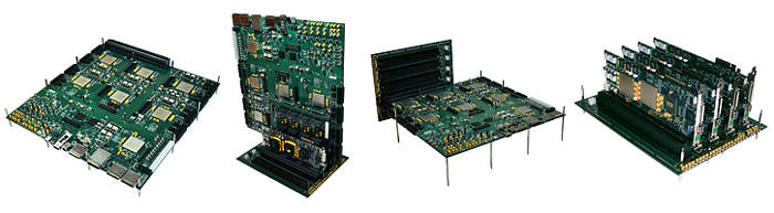
Aldec HES™ Prototyping Platform provides SoC/ASIC hardware and software developers with a high quality FPGA based HES boards utilizing the latest and largest FPGA chips - currently Xilinx® Virtex7® or UltraScale® families. It consists of large capacity multi-FPGA boards and is scalable from 8 to 633 Million ASIC gates by using backplane boards with fully utilized LVDS and GTH/GTX interconnections. Thus, it is ideal either for pre-silicon integration of the complete SoC or verification at the sub-system level.
The HES prototyping solution was architected to provide easy implementation and expansion while sustaining the highest performance and clock speeds sufficient for firmware and software development, debugging and SoC bring-up for all layers of the software stack including Android, Linux, Windows or RTOS operating systems and user level applications.
SoC Prototype Extension with Daughter Cards
The HES Prototyping Platform capabilities are extended with the rich portfolio of Daughter Cards that utilize high speed connectors which are either standard FMC HPC or BPX off-the-shelf MOLEX parts. Due to the use of non-proprietary connectors the daughter cards can be reused across different hardware platforms.
Each daughter card provides a unique set of devices and peripherals relevant to a given application, for instance:
- FMC-ADAS - designed to enable prototyping and evaluation of Automotive and Advanced Driver Assistance Systems designs.
- FMC-INTF - provides a good selection of commonly used peripherals like PCI Express, optical fiber QSFP+, Gigabit Ethernet, USB and more.
- FMC-IOT - provides a set of peripherals and interfaces commonly used in embedded designs of Internet-of-Things (IoT) applications.
- FMC-VISION - provides a set of multimedia interfaces for display panels, monitors and cameras
- FMC-NET & FMC-QSFP - provide high bandwidth networking interfaces
- FMC-INDUSTRY - commonly used industrial interfaces with industry grade parts
- HES7DB-SoC - provides ARM Cortex A9 dual-core CPU in a programmable Xilinx Zynq-7000 device and many other SoC targeted peripherals over BPX connector
- HES7DB-USB-ETH - provides USB 3/2/OTG Host and Hub and Gigabit Ethernet ports over BPX connector
Key Features & Benefits
- Scalable capacity up to 633 Million ASIC gates
- Up to 6 FPGA on a single board and scaled to 24 on the backplane configuration
- Fully utilized FPGA I/O for LVDS and GTX/GTH connectivity
- Advanced PCB design with perfect signals integrity and length aligned clock lines
- Extra large RAM capacity in SO-DIMM slots for DDR4 & DDR3
- Non-proprietary connectors for external peripherals and interfaces
- Host interface for FPGA programming, board configuration and diagnostics
- Reach choice of extension daughter cards
- Supports sub-systems prototyping and complete SoC integration
- Reusable for emulation and simulation acceleration by adding HES-DVM software
- Superior quality backed by industry leading 1-year warranty
Corporate Headquarters
2260 Corporate Circle
Henderson, NV 89074 USA
Tel: +1 702 990 4400
Fax: +1 702 990 4414
https://www.aldec.com
©2026 Aldec, Inc.