Diagnostic Design Configuration and Testing Using hes7proto.exe on the HES7XV690-4000BP board
Introduction
This application note describes how to configure and run Diagnostic Design on the HES-7 board using the hes7proto.exe application.
Spartan-6 FPGA Chip Preparation
Because the JTAG interface on the HES-7 board that is dedicated for 7-series FPGA chips must be functioning, the FPGA_PROG (Spartan-6) device needs to be configured correctly. It is recommended to run the FPGA_PROG configuration in case the user is not sure about the Spartan-6 configuration.
If your XCF32 PROM device is configured with the default hes7_spartan6.mcs file, or if your FPGA_PROG is configured with the hes7_spartan6.bit file, move to Kintex-7 and Virtex-7 Chips Configuration Using Standard USB Interface Connected to PC (Hes7proto.exe).
If your XCF32 PROM device and Spartan-6 chip are not configured properly or not configured at all, move to FPGA_PROG Chip Configuration.
NOTE: Aldec recommends using the default hes7_spartan6 files (.bit or .mcs) from: C:\Aldec\HES-7.Asic.Proto.2012.10.INCR_hes7_38637\spartan_firmware\implement as the default configuration files for your FPGA_PROG device.
FPGA_PROG Chip Configuration
Connect one side of the Aldec JTAG adapter to the CON2 connector on the HES-7 board.
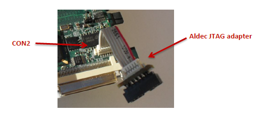
Figure 1 Aldec JTAG adapter connected to CON2 on the HES-7 board.
Connect the other side of the Aldec JTAG adapter to the Xilinx USB Platform cable connected to your PC.
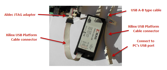
Figure 2 Aldec JTAG adapter connected to the Xilinx Platform USB cable.
Turn on the power supply for the HES7XV690-4000BP.
Initialize the JTAG chain for the Spartan-6 and XCF32 PROM devices on the HES-7 board using the Xilinx Impact programming tool.
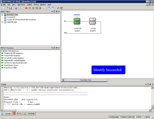
Figure 3 Spartan-6 JTAG chain successful initialization.
Configure the XCF32 PROM device with the hes7_spartan6.mcs file located within the C:\Aldec\HES-7.Asic.Proto.2012.10.INCR_hes7_38637\spartan_firmware\implement directory.
Reboot the board using the S1 tact switch, or by restarting the power supplier connected to the HES-7 board.
Spartan-6 will be configured automatically with the programming data stored in the PROM device after power-up.
NOTES:
PROM device is configured by default with the hes7_spartan.mcs file lcoated in the C:\Aldec\HES-7.Asic.Proto.2012.10.INCR_hes7_38637\spartan_firmware\implement directory.
Users can use the hes7_spartan6.bit file for direct FPGA chip configuration (when needed).
The HES-7 board should be rebooted after the PROM device configuration.
If the wrong configuration settings or the wrong bit file are used, the board may not work correctly.
Kintex-7 and Virtex-7 Chips Configuration Using Standard USB Interface Connected to PC (Hes7proto.exe)
Connect one side of the USB cable to the USB1 connector on the HES-7 board and the other side of the USB cable to the USB port in your PC.
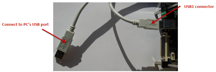
Figure 4 7-Series FPGAs JTAG chain successful initialization.
Turn on the power supply for the HES7xv690-4000BP.
Wait for the USB connection to initialize.
Run the hes7proto.exe --list command from the command line to make sure that the USB driver is installed and the HES-7 board is visible in your system.
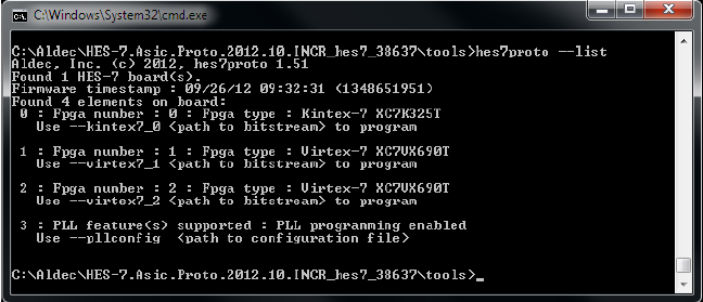
Figure 5 Correct result for hes7proto.exe --list.
From the command line, run the following for all FPGA chips programming with Diagnostic Design bits:
hes7proto.exe --kintex7_0 C:\Aldec\HES-7.Asic.Proto.2012.10.INCR_hes7_38637\diagnostic_design\lowspeed\top_fpga0.bit --virtex7_1 C:\Aldec\HES-7.Asic.Proto.2012.10.INCR_hes7_38637\diagnostic_design\lowspeed\top_fpga1.bit --virtex7_2 C:\Aldec\HES-7.Asic.Proto.2012.10.INCR_hes7_38637\diagnostic_design\lowspeed\top_fpga2.bit
NOTE: The example above assumes that hes7proto is installed on the default path
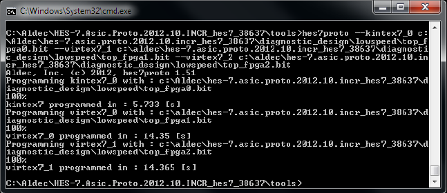
Figure 6 Correct result for 7-Series FPGA chips programmed using the hes7proto.exe application.
Kintex-7 and Virtex-7 Chips Testing – Diagnostic Design Using hes7proto.exe
Before starting HES-7 Diagnostic Design, the HES-7 FPGA chips need to be connected to the USB port in your PC and configured correctly.
FPGA_PROG needs to be configured with the default hes7_spartan6.bit file from the C:\Aldec\HES-7.Asic.Proto.2012.10.INCR_hes7_38637\spartan_firmware\implement directory.
FPGA0 needs to be configured with the top_fpga0.bit file from the C:\Aldec\HES-7.Asic.Proto.2012.10.INCR_hes7_38637\diagnostic_design\lowspeed directory.
FPGA1 needs to be configured with the top_fpga1.bit, file from the C:\Aldec\HES-7.Asic.Proto.2012.10.INCR_hes7_38637\diagnostic_design\lowspeed directory.
FPGA2 needs to be configured with the top_fpga2.bit file from the C:\Aldec\HES-7.Asic.Proto.2012.10.INCR_hes7_38637\diagnostic_design\lowspeed directory.
Diagnostic Design Testing Procedure
Run the hes7proto.exe --list command in the command line to make sure that the USB driver is installed and the HES-7 board is visible in your system.
Run the hes7proto.exe --reset --status commands from the command line to reset the FPGA0-2 designs and check the status of the Diagnostic Design test.
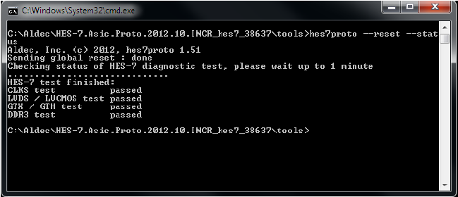
Figure 7 Correct result for hes7proto.exe --reset --status commands
Corporate Headquarters
2260 Corporate Circle
Henderson, NV 89074 USA
Tel: +1 702 990 4400
Fax: +1 702 990 4414
https://www.aldec.com
©2026 Aldec, Inc.