SW2 DIP Switch and LED1-8 bar LEDs on the HES7XV690-4000BP Board
Introduction
This application note describes all of the possible configurations of the S2 DIP switch that is available for Diagnostic Design that is delivered with the HES7XV690-4000BP board.
The following sections also present status codes that are available on the LED1-8 bar LED indicators.
HES7XV690-4000BP S2 DIP switch description
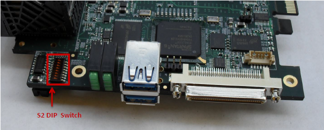
Figure 1 S2 DIP Switch location
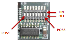
Figure 2 S2 DIP Switch orientation
Table 1: S2 DIP Switch Description Table |
||
DIP Switch position |
Function |
Description |
POS1 |
HARD RESET |
Turning On this switch causes loss of FPGA0-2 configurations |
POS2 |
USER RESET |
Turning ON this switch causes a reset of the user designs in the FPGA0-2 chips |
POS3 |
Bar LEDs status selector |
POS3-5 switches between statuses from FPGA0, FPGA1, FPGA2, PLLs, and the master status from Diagnostic Design |
POS4 |
||
POS5 |
||
POS6 |
PLLs control selector |
Selects PLLs control master between the USB program and Diagnostic Design |
POS7 |
PLLs conf. selector |
Switches between PLLs configuration type (High/Low speed) that is intended for Diagnostic Design |
POS8 |
PLLs Reset |
PLLs chip reset - must be issued after configuration or PLLs selector change |
S2 DIP Switch Configuration Tables
Table 2: S2 DIP Switch, POS1 Configuration Table |
|
POS1 |
Description |
ON |
HARD RESET active - FPGA0-2 lost their configurations |
OFF (default) |
HARD RESET inactive - normal operations |
Table 3: S2 DIP Switch, POS2 Configuration Table |
|
POS2 |
Description |
ON |
USER RESET active- reset signal for test design located in FPGA0-2 |
OFF (default) |
USER RESET inactive - normal operations |
Table 4: S2 DIP Switch, POS3-5 Configuration Table |
|||
POS3 |
POS4 |
POS5 |
Description |
ON |
ON |
ON |
Eight user statuses from FPGA0 |
OFF |
ON |
ON |
Eight user statuses from FPGA1 |
ON |
OFF |
ON |
Eight user statuses from FPGA2 |
OFF |
OFF |
ON |
Six statuses from PLLs SI5326 - locked signals |
ON |
ON |
OFF |
Six statuses from I2C configuration module - error NACK signals |
OFF |
ON |
OFF |
Three statuses of DONE signals from FPGAs |
OFF |
OFF |
OFF |
Five statuses from Diagnostic Design |
(default) |
|||
Table 5: S2 DIP Switch, POS6 Configuration Table |
|
POS6 |
Description |
ON |
PLL control from USB program |
OFF (default) |
Internal PLL control from Diagnostic Design |
Table 6: S2 DIP Switch, POS7 Configuration Table |
|
POS7 |
Description |
ON |
PLL internal configuration1 – used for High Speed Diagnostic design |
OFF (default) |
PLL internal configuration2 – used for Low Speed Diagnostic design |
Table 7: S2 DIP Switch, POS8 Configuration Table |
|
POS8 |
Description |
ON |
PLL Reset active |
OFF (default) |
PLL Reset inactive |
LED1-8 Status Bar LEDs Description
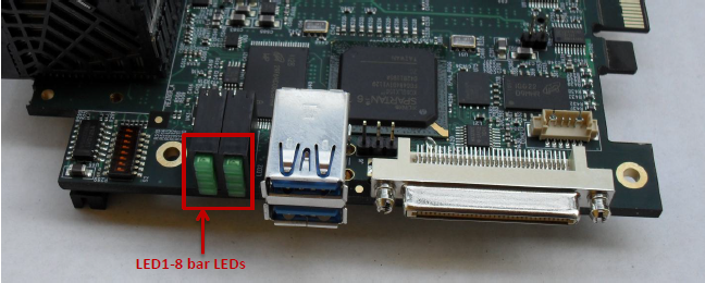
Figure 3 LED1-8 status bar LEDs location
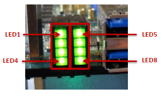
Figure 4 LED1-8 bar LEDs indicators
Diagnostic Design LED1-8 Bar LEDs statuses
Table 8: Bar LEDs status for Diagnostic Design Test (POS3, POS4, POS5=OFF, OFF, OFF) |
||||
Description |
LED |
Description |
||
Clocking test succeeded (when ON) |
LED1 |
LED5 |
Empty |
|
Interconnections test succeeded (when ON) |
LED2 |
LED6 |
Empty |
|
GTX/GTH test succeeded (when ON) |
LED3 |
LED7 |
Empty |
|
Memory test succeeded (when ON) |
LED4 |
LED8 |
Diagnostic Design is working (when blink) |
|
Table 9: Default S2 DIP Switch Settings for Diagnostic Design Test |
|||||||
POS1 |
POS2 |
POS3 |
POS4 |
POS5 |
POS6 |
POS7 |
POS8 |
OFF |
OFF |
OFF |
OFF |
OFF |
OFF |
OFF |
OFF |
Table 10: Default LED1-8 Bar LEDs Statuses for FPGA2 Test |
||||
State |
LED |
State |
||
ON |
LED1 |
LED5 |
OFF |
|
ON |
LED2 |
LED6 |
OFF |
|
ON |
LED3 |
LED7 |
OFF |
|
ON |
LED4 |
LED8 |
Blink |
|
Diagnostic Design tests description:
Memory test - SO-DIM memories test
GTX/GTH test - all GTX/GTH connections test
Interconnections test - all IO interconnections (all available connections between FPGA0-2) test
Clocking test - clock module and clock lines test
NOTE: The Diagnostic test takes about 30 seconds and is signalized by the blinking of LED8
LED1-8 Bar LEDs statuses for FPGA0
Table 11: Bar LEDs status for FPGA0 (POS3, POS4, POS5=ON, ON, ON) |
||||
Description |
LED |
Description |
||
REF clk present (when BLINK) |
LED1 |
LED5 |
GTX from FPGA1 to FPGA0 fail (when ON) |
|
Clock test fail (when ON) |
LED2 |
LED6 |
Empty |
|
LVDS from FPGA1 to FPGA0 fail (when ON) |
LED3 |
LED7 |
DDR status1* |
|
Common bus fail (when ON) |
LED4 |
LED8 |
DDR status2* |
|
*refer to Table 12: DDR status1-2 |
||||
Table 12: DDR Status1-2 |
||
DDR status1 |
DDR status2 |
Description |
OFF |
OFF |
no errors |
OFF |
ON |
Incorrect SO-DIMM module for the test (SPD parameters not valid) |
ON |
OFF |
Calibration failed |
ON |
ON |
Data error present |
Table 13: Default S2 DIP Switch Settings for FPGA0 Test |
|||||||
POS1 |
POS2 |
POS3 |
POS4 |
POS5 |
POS6 |
POS7 |
POS8 |
OFF |
OFF |
ON |
ON |
ON |
OFF |
OFF |
OFF |
Table 14: Default LED1-8 bar LEDs statuses for FPGA2 Test |
||||
State |
LED |
State |
||
BLINK |
LED1 |
LED5 |
OFF |
|
OFF |
LED2 |
LED6 |
OFF |
|
OFF |
LED3 |
LED7 |
OFF |
|
OFF |
LED4 |
LED8 |
OFF |
|
LED1-8 Bar LEDs Statuses for FPGA1
Table 15: Bar LEDs status for FPGA1 (POS3, POS4, POS5=OFF, ON, ON) |
||||
Description |
LED |
Description |
||
REF clk present (when BLINK) |
LED1 |
LED5 |
GTX from FPGA0 to FPGA1 fail (when ON) |
|
Clock test fail (when ON) |
LED2 |
LED6 |
GTX from FPGA2 to FPGA1 fail (when ON) |
|
LVDS from FPGA0 to FPGA1 fail (when ON) |
LED3 |
LED7 |
DDR status1* |
|
LVDS from FPGA2 to FPGA1 fail (when ON) |
LED4 |
LED8 |
DDR status2* |
|
*refer to Table 16: DDR status1-2 |
||||
Table 16: DDR Status1-2 |
||
DDR status1 |
DDR status2 |
Description |
OFF |
OFF |
no errors |
OFF |
ON |
Incorrect SO-DIMM module for the test (SPD parameters not valid) |
ON |
OFF |
Calibration failed |
ON |
ON |
Data error present |
Table 17: Default S2 DIP Switch Settings for FPGA2 Test |
|||||||
POS1 |
POS2 |
POS3 |
POS4 |
POS5 |
POS6 |
POS7 |
POS8 |
OFF |
OFF |
OFF |
ON |
ON |
OFF |
OFF |
OFF |
Table 18: Default LED1-8 bar LEDs statuses for FPGA2 Test |
||||
State |
LED |
State |
||
BLINK |
LED1 |
LED5 |
OFF |
|
OFF |
LED2 |
LED6 |
OFF |
|
OFF |
LED3 |
LED7 |
OFF |
|
OFF |
LED4 |
LED8 |
OFF |
|
=H2 LED1-8 Bar LEDs Statuses for FPGA2
Table 19: Bar LEDs status for FPGA1 (POS3, POS4, POS5=ON, OFF, ON) |
||||
Description |
LED |
Description |
||
REF clk present (when BLINK) |
LED1 |
LED5 |
Empty |
|
Clock test fail (when ON) |
LED2 |
LED6 |
GTX from FPGA1 to FPGA2 fail (when ON) |
|
Common bus fail (when ON) |
LED3 |
LED7 |
Empty |
|
LVDS from FPGA1 to FPGA2 fail (when ON) |
LED4 |
LED8 |
Empty |
|
Table 20: Default S2 DIP Switch Settings for FPGA2 Test |
|||||||
POS1 |
POS2 |
POS3 |
POS4 |
POS5 |
POS6 |
POS7 |
POS8 |
OFF |
OFF |
ON |
OFF |
ON |
OFF |
OFF |
OFF |
Table 21: Default LED1-8 bar LEDs statuses for FPGA2 Test |
||||
State |
LED |
State |
||
BLINK |
LED1 |
LED5 |
OFF |
|
OFF |
LED2 |
LED6 |
OFF |
|
OFF |
LED3 |
LED7 |
OFF |
|
OFF |
LED4 |
LED8 |
OFF |
|
LED1-8 Bar LEDs Statuses for PLLs Lock Test
Table 22: Bar LEDs status for PLLs Configuration Test (POS3, POS4, POS5=OFF, OFF, ON) |
||||
Description |
LED |
Description |
||
CLK0 PLL locked (when ON) |
LED1 |
LED5 |
CLK_PLL PLL locked (when ON) |
|
CLK1 PLL locked (when ON) |
LED2 |
LED6 |
CLK_GTX PLL locked (when ON) |
|
CLK2 PLL locked (when ON) |
LED3 |
LED7 |
Empty |
|
CLK3 PLL locked (when ON) |
LED4 |
LED8 |
Empty |
|
Table 23: Default S2 DIP Switch Settings for PLLs Lock Test |
|||||||
POS1 |
POS2 |
POS3 |
POS4 |
POS5 |
POS6 |
POS7 |
POS8 |
OFF |
OFF |
OFF |
OFF |
ON |
OFF |
OFF |
OFF |
Table 24: Default LED1-8 bar LEDs statuses for PLL Lock Test |
||||
State |
LED |
State |
||
ON |
LED1 |
LED5 |
ON |
|
ON |
LED2 |
LED6 |
ON |
|
ON |
LED3 |
LED7 |
OFF |
|
ON |
LED4 |
LED8 |
OFF |
|
LED1-8 Bar LEDs Statuses for PLLs Configuration Test
Table 25: Bar LEDs status for PLLs Configuration Test (POS3, POS4, POS5=ON, ON, OFF) |
||||
Description |
LED |
Description |
||
CLK0 PLL configuration error (when ON) |
LED1 |
LED5 |
CLK_PLL PLL configuration error (when ON) |
|
CLK1 PLL configuration error (when ON) |
LED2 |
LED6 |
CLK_GTX PLL configuration error (when ON) |
|
CLK2 PLL configuration error (when ON) |
LED3 |
LED7 |
Empty |
|
CLK3 PLL configuration error (when ON) |
LED4 |
LED8 |
Empty |
|
Table 26: Default S2 DIP Switch Settings for PLLs Configuration Test |
|||||||
POS1 |
POS2 |
POS3 |
POS4 |
POS5 |
POS6 |
POS7 |
POS8 |
OFF |
OFF |
ON |
ON |
OFF |
OFF |
OFF |
OFF |
Table 27: Default LED1-8 bar LEDs statuses for PLL Configuration Test |
||||
State |
LED |
State |
||
OFF |
LED1 |
LED5 |
OFF |
|
OFF |
LED2 |
LED6 |
OFF |
|
OFF |
LED3 |
LED7 |
OFF |
|
OFF |
LED4 |
LED8 |
OFF |
|
LED1-8 Bar LEDs Statuses for FPGAs done signals
Table 28: Bar LEDs status for FPGAs done signals (POS3, POS4, POS5=OFF, ON, OFF) |
||||
Description |
LED |
Description |
||
FPGA0 Done signal (when ON) |
LED1 |
LED5 |
Empty |
|
FPGA1 Done signal (when ON) |
LED2 |
LED6 |
Empty |
|
FPGA2 Done signal (when ON) |
LED3 |
LED7 |
Empty |
|
Empty |
LED4 |
LED8 |
Empty |
|
Table 29: Default S2 DIP Switch Settings for FPGAs Done signals |
|||||||
POS1 |
POS2 |
POS3 |
POS4 |
POS5 |
POS6 |
POS7 |
POS8 |
OFF |
OFF |
OFF |
ON |
OFF |
OFF |
OFF |
OFF |
Table 30: Default LED1-8 bar LEDs statuses for FPGAs Done signals |
||||
State |
LED |
State |
||
ON |
LED1 |
LED5 |
OFF |
|
ON |
LED2 |
LED6 |
OFF |
|
ON |
LED3 |
LED7 |
OFF |
|
OFF |
LED4 |
LED8 |
OFF |
|
Corporate Headquarters
2260 Corporate Circle
Henderson, NV 89074 USA
Tel: +1 702 990 4400
Fax: +1 702 990 4414
https://www.aldec.com
©2026 Aldec, Inc.