HES Proto-AXI Interconnect
FPGA boards are proving increasingly popular in a variety of sectors and for varied applications. For instance, they can be used for ASIC and SoC prototyping, for accelerating algorithms in high performance computing (HPC), for hardware-accelerated computer vision, and for high frequency trading (HFT) on the stock markets.
Typically, the FPGA is not a stand-alone component. Rather, it works with another machine, which will be called the Host in this article, and communication is via a Host-FPGA bridge.
There are also some other hardware resources on the FPGA board such as external memories (DDR, QDR, RLD) and/or high-speed networking interfaces (like QSFP) that often play a key role in the application and which require reliable and robust controllers in the FPGA.
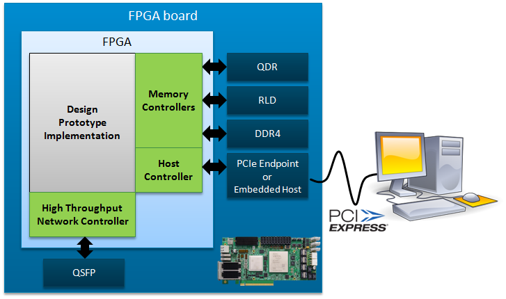
Designing the host bridge and peripheral controllers is not an easy task and takes a considerable amount of time; time that could be better spent on the development of core functionality and innovative features.
Addressing these needs, Aldec provides HES Proto-AXI™ Interconnect, a complete and ready-to-use external connectivity and bridge solution. Our HES Proto-AXI is based on the AMBA AXI4 bus standard and facilitates the quick integration of the design in FPGA, with either an external host computer or an embedded ARM Cortex host and various types of on-board memory components. Besides standardized and universal AXI4 interface, the HES Proto-AXI has a high bandwidth and low latency link enabling fast DMA data transfers between software and hardware; reaching a throughput of 10GB/s for read and 5.5GB/s for write operations over PCI Express gen4.
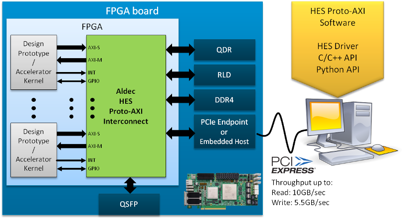
Our HES Proto-AXI allows for the connection of multiple design modules or algorithm accelerator that can be both master and/or slave types of AXI4 memory-mapped devices. All these devices can transfer data with one another and to on-board memory thanks to an AXI interconnect contained in the HES Proto-AXI module.
The memory map of AXI Interconnect can be modified via address remappers. There are also GPIO and Interrupt (INT) lanes included in the HES Proto-AXI IP that can be used to implement non-standard interfaces or to transfer notifications, status or configuration data to software without using AXI protocol. The largest designs, especially those in the large scale HPC applications, will benefit from multi-FPGA and multi-board support.
Key Features & Benefits
- Host and external memory interface based on widely adopted AMBA AXI4 standard
- GPIO and Interrupts extend base AMBA AXI functionality
- PCI Express-based, high throughput Workstation Host type interface
- Low latency and high throughput Embedded Host type interface
- Complete one-board prototype and test solution utilizing ARM Cortex processors
- Allows building software driven testbenches or portable prototypes
- Reduces overhead of host and memory interface implementation
- Supports connecting multiple design modules or algorithm kernels
- Scalable solution with support of multiple FPGAs and multiple HES boards connected in one host
- Easy to use software API available for C/C++ and Python developers
Deliverables
- HES Proto-AXI IP modules:
- Interconnect mode supports multiple AXI Master & Slave design modules, memories, and host bridge
- Bridge mode supports single AXI Slave design module and host bridge
- Software API in C/C++ and Python
- Simulation models in SystemVerilog with DPI-C proxy to software API
- Linux & MS Windows PCIe Driver for Workstation Host type
- Embedded Linux for Embedded Host type
- Examples & User Guide
Corporate Headquarters
2260 Corporate Circle
Henderson, NV 89074 USA
Tel: +1 702 990 4400
Fax: +1 702 990 4414
https://www.aldec.com
©2026 Aldec, Inc.