ARM Cortex Support
HES™ supports ARM® dual-core Cortex™-A9 MPCore™ with Xilinx® Zynq™-7000 MPSoC, enabling designers to leverage the serial processing capabilities of the Cortex-A9 processor for applications that require intensive computations with the parallel processing capabilities of HES ASIC prototyping platform to create applications across a diverse range of markets including: Video, Vision, Communications, Control Systems and Bridging.
The 8 to 633 million ASIC gate scalable capacity of HES, coupled with open-source Linux, Android, and FreeRTOS solutions available from Xilinx, delivers a powerful verification platform for combined hardware and software design teams. Depending on the design size, functional and PHY requirements the Zynq MPSoC can be incorporated in two distinctive configurations:
Single-board solution with HES-US-440
The board HES-US-440 combines the largest Virtex Ultrascale FPGA XCVU440 with the largest Xilinx Zynq-7000 MPSoC XC7Z100 on a single PCB board that allows building a self contained, single-board embedded testbench or implementing other prototypes that require CPU based controller.
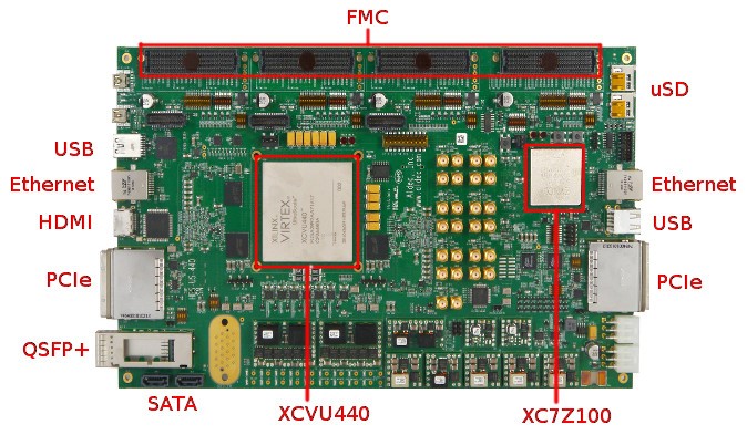
HES-US-440 Key Features:
- 26 million gates FPGA capacity in a single Virtex UltraScale XCVU440 FPGA
- Scalable to 52 million gates (2x HES-US-440 connected via FMC interconnect board)
- ARM Cortex in the Zynq-7000 XC7Z100 MPSoC FPGA
- On-board peripherals USB, Ethernet, PCIe, SATA, QSFP+
- On-board memories DDR4, DDR3, RLDRAM-3, SPI Flash, NAND Flash, microSD
- Standardized FMC extension connectors and available daughter cards
- Open-source Linux, Android, and FreeRTOS solutions available from Xilinx
Related blog article: Software Driven Test of FPGA Prototype
Extension Daughter Card - HES7DB-SoC
The daughter card HES7DB-SoC extends the capabilities of HES boards by providing the ARM Cortex A9 dual-core CPU in a programmable Xilinx Zynq-7000 device and additional peripherals that are commonly used in SoC designs. It contains the full size BPX connector which enables many configurations with both HES-7 and HES-US base boards to support design sizes from 8 to 633 million ASIC gates.

HES7DB-SoC Key Features:
- Xilinx Zynq-7000 module (XC7Z045-FFG676), dual core ARM Cortex A9 MPCore
- Media Interfaces – Ethernet PHY 10/100/1000, Wi-Fi and Bluetooth, USB 2.0 DEVICE, USB 2.0 HOST, USB 2.0 OTG, HDMI, and Audio Codec (Stereo Speaker and MIC Interfaces)
- Memories – DDR3, SO-DIMM DDR2, SD Socket, SPI Flash, NAND Flash, I2C Flash
- Connectors – ARM Debug, RS232, I2C, SPI, and GPIO
- Open-source Linux, Android, and FreeRTOS solutions available from Xilinx
Recorded Webinar: ARM Cortex SoC Prototyping Platform for Industrial Applications
Learn how to tackle industrial design applications with HES-7™, which supports ARM® Cortex™-A9 based designs by leveraging Xilinx® Zynq® All Programmable SoC.
Corporate Headquarters
2260 Corporate Circle
Henderson, NV 89074 USA
Tel: +1 702 990 4400
Fax: +1 702 990 4414
https://www.aldec.com
©2026 Aldec, Inc.