

Top Features
- Supported Microchip devices/capacities: RTAX-S/SL up to 4000S, RTSX-SU, and RTAX-D devices
- Automated Device Netlist Converter:
- Memory Conversion
- Physical Design Constraint (PDC) file conversion
- Compatible with Linux and Windows OS
- Simulation capability with Riviera-PRO

Microchip ProASIC®3E FPGA Technology
Using ProASIC3E FPGA flash-based programming technology instead of traditional OTP anti-fuse space-qualified FPGAs (AX chips) provides significant advantages, such as a smaller device size with greater routing flexibility, more switches, lower power consumption, non-volatile re-programmability with easier technology mapping and Netlist optimizations. The Microchip ProASIC3E FPGA family supports devices from 15,000 to 3 million ASIC gates and includes 504Kbits of true dual-port SRAM, 620 user I/Os, 1KB of flash-ROM and provides secure IP 128-bit AES encryption/decryption.
Aldec Re-Programmable Prototyping Adaptors
The Aldec prototyping adaptor board maps the footprint of the Microchip ProASIC3E FPGA device to the footprint of the Microchip RTAX-S/SL or RTSX-SU device (e.g. CQ208, CQ256, CQ352, CG624, CG1152 or CG1272). After soldering the adaptor to the PCB, a programming connector (JTAG) provides on-the-fly reprogramming of the device, without detaching the adaptor from the target PCB. In addition, a GUI-based EDIF Netlist Converter Application, is available for automatic pin re-mapping from anti-fuse to flash-based architecture. Aldec prototyping adaptors are available today, in a wide-variety of supported device capacities and packages.
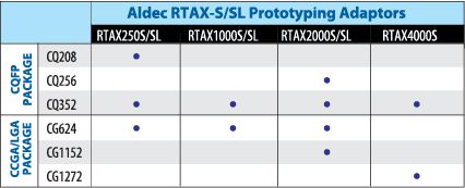
RTAX-S/SL Prototyping Adaptors


- Microchip ProASIC3E device
- JTAG connector
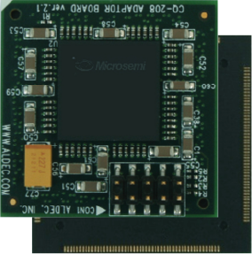
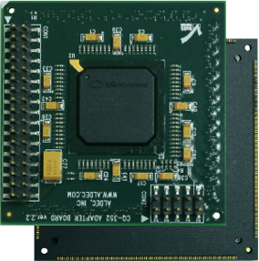
- CQ208 footprint
- Size: 37mm x 37mm

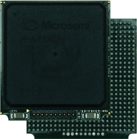
- Microchip ProASIC3E device
- JTAG connector
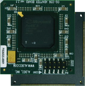
- CQ256 footprint
- Size: 43.07mm x 43.07mm

- Microchip ProASIC3E device Commercial or Industrial
- JTAG connector
- Power connector
- CQ352 footprint
- Size: 55mm x 55mm

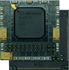
- Microchip ProASIC3E device Commercial or Industrial
- JTAG connector
- CG624 footprint
- Size: 32.5mm x 34mm
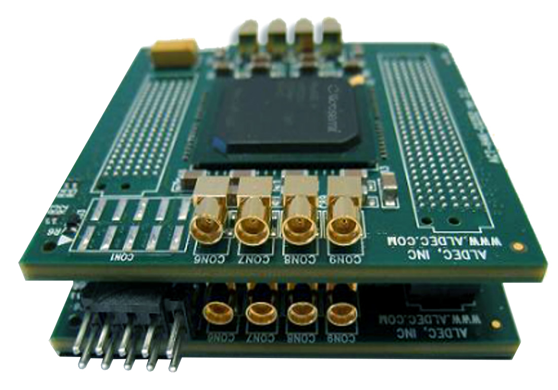

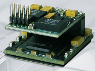
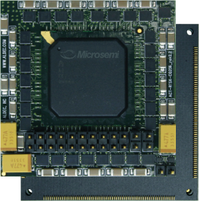
- Stacked MB/DB with:
- Microchip ProASIC3E device
- JTAG connector
- CQ352 footprint
- Size: 55mm x 55mm


- Microchip RTG4 or Polarfire device
- DSP 462 / DSP 1480
- JTAG connector
- CQ352 footprint
- Size: 55mm x 55mm
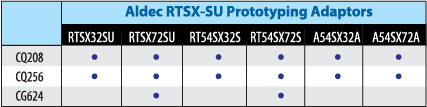
RTSX-SU Prototyping Adaptors

- Microchip ProASIC3E device
- JTAG connector
- CQ208 footprint
- Size: 37mm x 37mm

- Microchip ProASIC3E device
- JTAG connector
- CQ256 footprint
- Size: 43.07mm x 43.07mm

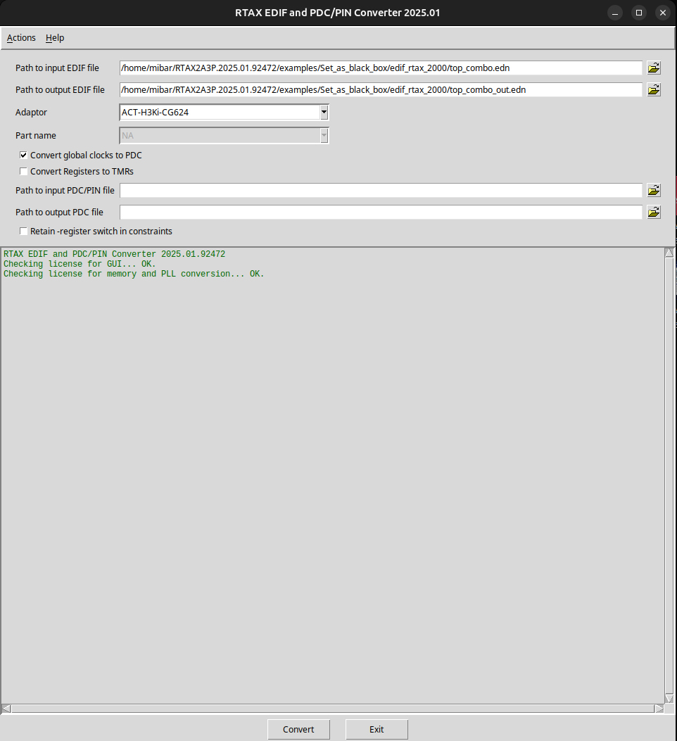
EDIF Netlist Converter
The RTAX EDIF Netlist Converter, an optional application, performs automatic conversion of the RTAX-S/SL and RTSX-SU EDIF netlist to a ProASIC3E netlist, taking into consideration the differences between RTAX-S/SL or RTSX-SU anti-fuse and ProASIC3E flash-based technologies.
A pin re-mapping utility provides automatic Physical Design Constraint (PDC) file conversion, which eliminates the need for additional, time consuming manual work.
New Solutions
- Custom Adaptor: RTG4 / RTPolarFire
- Custom eval boards for Adaptors
- 3D printed RT Covers
- MX Chips support: A42MX32
RTAX/RTSX Adaptor Boards Inquiry
Corporate Headquarters
2260 Corporate Circle
Henderson, NV 89074 USA
Tel: +1 702 990 4400
Fax: +1 702 990 4414
https://www.aldec.com
©2026 Aldec, Inc.