HES-VU19PD-ZU7EV
Capacity
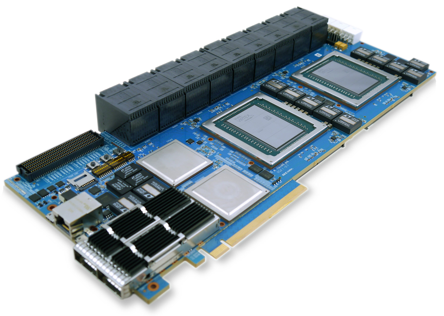
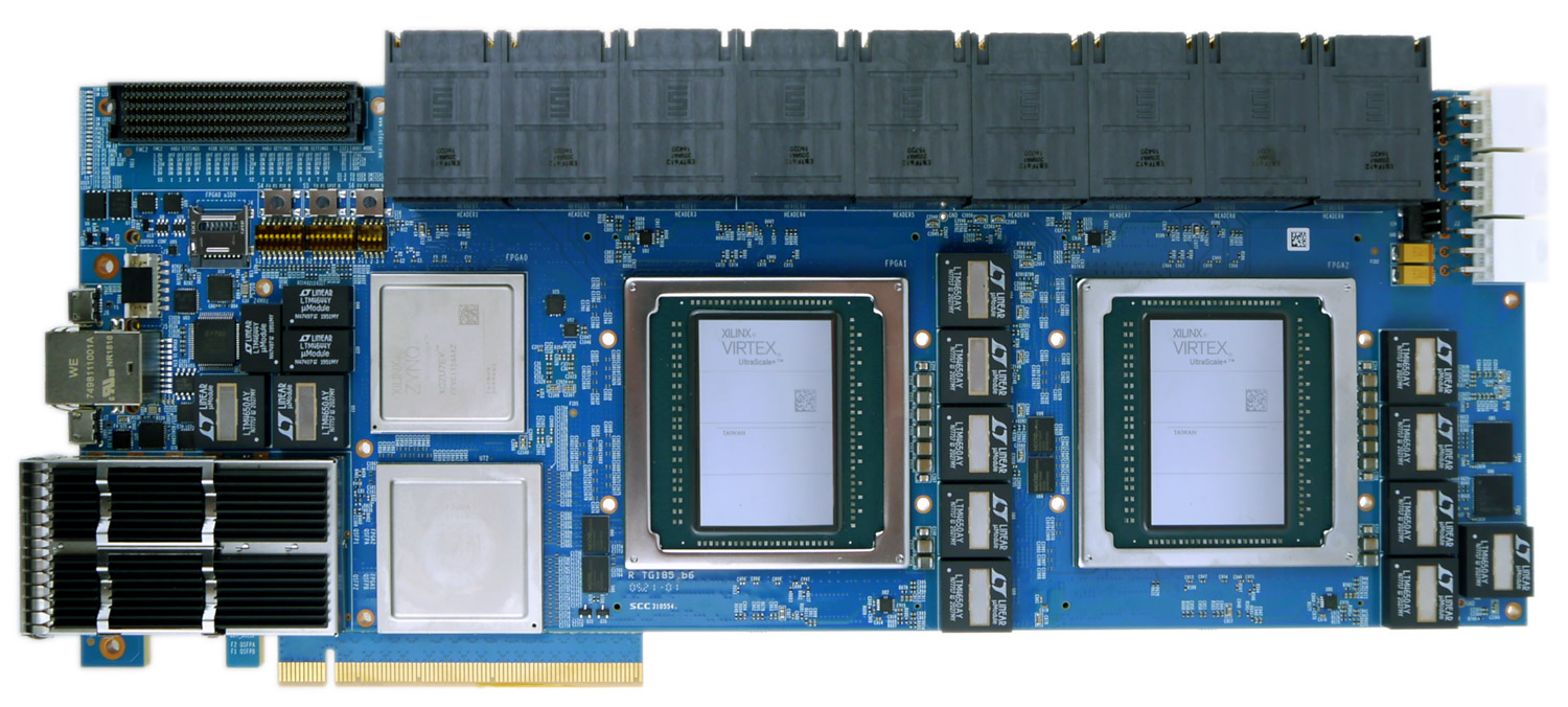
The HES-VU19PD-ZU7EV offers a unique combination of two Virtex UltraScale+ VU19P FPGAs as logic module and one Xilinx Zynq UltraScale+ ZU7EV MPSoC as the host module that features a Quad-core ARM® Cortex-A53, Dual-core ARM® Cortex-R5 real-time processing units, an ARM® Mali-400 MP2 GPU, integrated H.264/H.265 video codec, and UltraScale+™ programmable logic in a 16nm FinFET node. This board is targeted for high-speed physical prototyping and emulation of medium to large ASIC designs. The HES-VU19PD-ZU7EV provides 83M ASIC gates and it goes up to 316M gates on a backplane.
There are 5x SODIMM external memory available on the board, 4x are connected to VU19P devices and 1x connected to the ZU7EV device. On chip memory for the VU19P device is 166Mb and 11Mb for the ZU7EV device.
| Resources | VU19P Virtex UltraScale+™ FPGA |
ZU7EV Zynq UltraScale+™ MPSoC | |
| Logic Cells/LUTs (K) | 8,938 | 504 | |
| Total Block RAM (Mb) | 75.9 | 11 | |
| UltraRAM (Mb) | 90 | 27 | |
| DSP Slices | 3840 | 1728 | |
| Transceivers | 80 GTY (32.75 Gb/s) | 20 GTH (16.3Gb/s) | |
| I/O | 1664 HP, 96 HD | 214 PS, 312 HP, 48 HD | |
Clocking
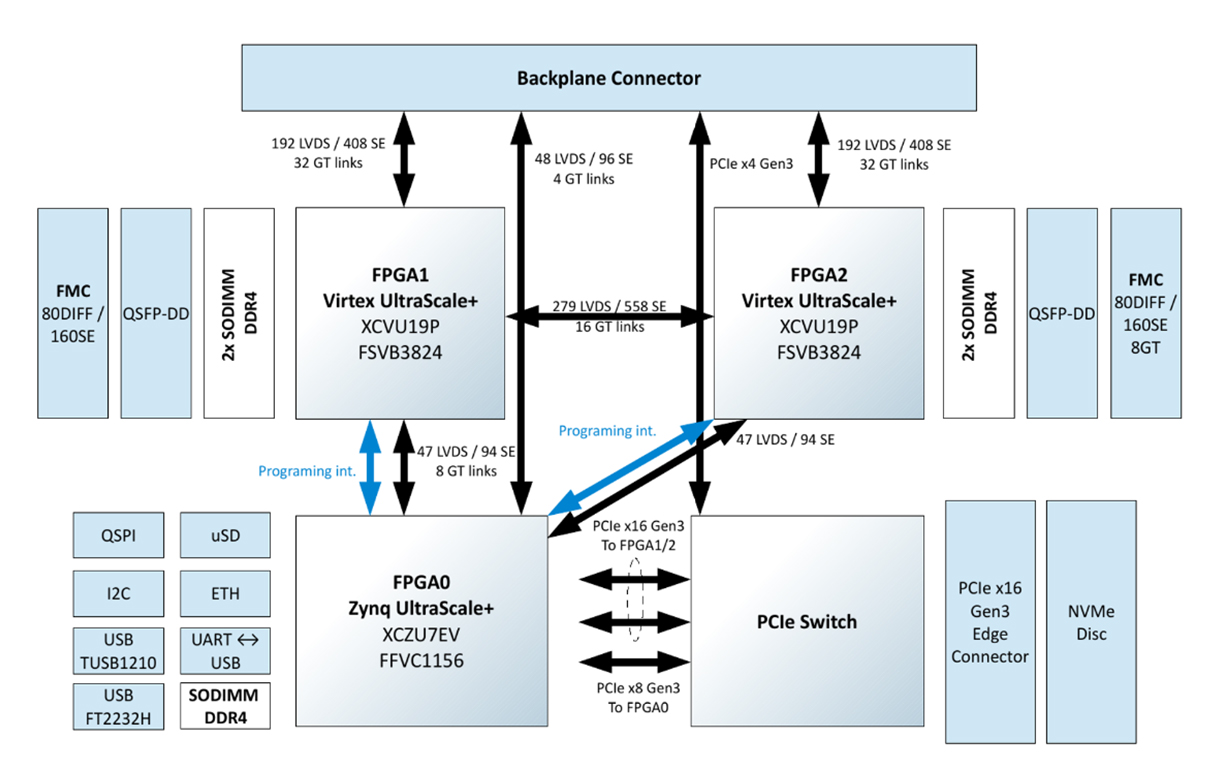
There are two configurable clock generators (PLL), two reference clocks for FPGA0-2 (XCZU7EV) GTH transceivers, two reference oscillators 100MHz and 200MHz for FPGA0-2, 400 MHz reference oscillator for FPGA1-2 (XCVU19P) and a reference oscillator connected to FPGA1-2 dedicated for SODIMM memory on HES-XCVU19PD-ZU7EV board. Additionally, there are six clock buffers on board that allow the distribution of clocks between FPGA0-2, FMC, and BP connectors.
Hosting & Interfaces
The board is connected to a workstation or server through the board’s PCIe x16 edge connector. A wide variety of interfaces are available to be connected to the FPGA devices.
| Interfaces | |
| Virtex® UltraScale+™ VU19P FPGA | Zynq® UltraScale+™ ZU7EV MPSoC (connected to the ARM® processing system) |
|
|
Other than the FPGAs on the board, there is PCIe switch device responsible for preparing the communication between all connected devices (Zynq and VU19P devices) and the NVMe SSD card. It is connected to VU19P FPGAs with 16 links, to Zynq MPSoC with 8 links, and to backplane connector with PCIe x4 Gen3.
Aldec provides the HES Proto-AXI software package with necessary drivers and utilities for programming and communication with the board. For quick bring-up of host connection, Aldec provides ready to use image of the embedded Linux for ZU7EV device and HES Proto-AXI solution, which consists of a bridge module IP with AMBA AXI interface and accompanying PCI Express HES driver with C++ API for Linux and Windows PC allowing to transfer data directly to the AMBA AXI local bus behind the bridge. HES-VU19PD-ZU7EV supports HES Proto-AXI embedded mode by which the board can function in standalone mode without PCIe connection with the workstation. Power is supplied by a standard 6-pin PCIe power cable.
HES-VU19PD-ZU7EV
FPGA & Capacity
- Main FPGA: 2x Virtex UltraScale+ XCVU19P-FSVB3824 (1664 HP, 96 HD and 80 GTY)
- ASIC Gates estimated:
- 83 Million Gates single board
- 332 Million Gates with four boards in a backplane
- Host FPGA: Zynq UltraScale+ XCZU7EV-FFVC1156 (214 PS, 312 HP, 48 HD)
Flexible Clocking
- Two configurable clock generators (PLL) provide 2 clocks for FPGA0-FPGA2 and backplane and 2 clocks for FPGA1-FPGA2 and backplane
- Two reference oscillators 100MHz and 200MHz for FPGA0-FPGA2
- 400MHz reference oscillators for FPGA1-FPGA2
- 200MHz reference oscillator for SODIMM memory to FPGA1-2
- Six clock buffers (distribution clocks between FPGA, FMC and backplane connectors)
- Two reference clocks for GT links
- Additional dedicated clock source for PCIe and QSFP interfaces
Connectivity & Expandability
- Full size backplane connector
- Daughter card connectors (FMC-HPC)
- Standard FPGA Mezzanine Card connectors
- Compliant with ANSI/VITA 57.1 FMC Standard
- 2 FMC sockets connected to UltraScale+ FPGAs
- FMC1 (80 DIFF / 160 SE, 8 GT)
- FMC2 (80 DIFF / 160 SE)
- Inter-FPGA connections
- UltraScale interconnections
- 279 Diff - standard GPIO optimized for LVDS
- 16 GT - high speed serial I/O
- UltraScale to ZU7EV host FPGA connections
- 47 Diff - standard GPIO optimized for LVDS
- 8 GT - high speed serial I/O
- GPIO & Misc
- 4x USER LEDs
Memory Resources
- Up to 64 GB of DDR4
- 4 DDR4 SO-DIMM slots
- 2 slots and up to 16 GB per VU19P
- Memories connected to Zynq MPCoC UltraScale+
- 1 SO-DIMM slot
- QSPI Flash
- Micro-SD slot for memory to store FPGA configuration bit-files
- NVMe disc interface (connected to FPGA0-FPGA2 via pcie switch
Interfaces & Hosting
- Host interfaces at VU19P
- PCIe interface for each FPGA
- Fixed PCIe x16 gen3
- PCIe Switch
- 2x QSFP-DD
- Interfaces at ZU7EV
- uSD
- 1 Gb Ethernet
- UART
- USB
- I2C
- Board configuration and FPGA programming
- Aldec’s Board Configuration Controller loaded in Zynq ZU7EV
- Programming from Host
- via USB 2.0 (Aldec HES Proto-AXI application)
- via JTAG (Xilinx utilities)
- Programming from Micro-SD card
Corporate Headquarters
2260 Corporate Circle
Henderson, NV 89074 USA
Tel: +1 702 990 4400
Fax: +1 702 990 4414
https://www.aldec.com
©2026 Aldec, Inc.