HES-XCKU11P-DDR4
Capacity
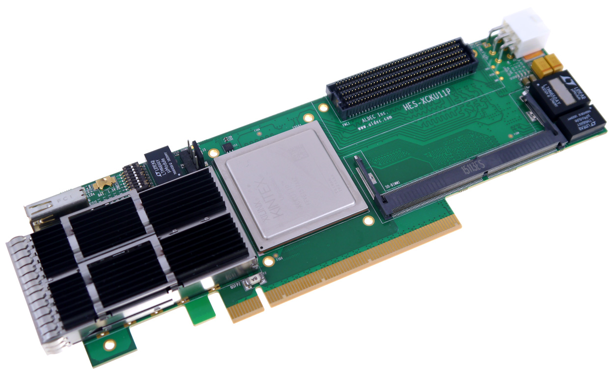
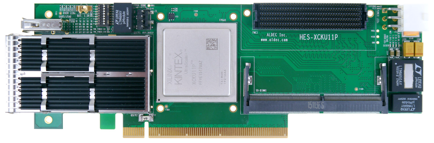
The HES-XCKU11P-DDR4 contains Kintex UltraScale+ XCKU11P FPGA belonging to the family of chips from Xilinx which provide the best price/performance/watt balance. Two QSFP-DD can provide high bandwidth and low-latency communication (up to 400 Gbps). Thanks to the SO-DIMM memory socket there is available to connect external high-speed DDR4 memory module. FMC connector compliant with ANSI/VITA 57.1 standard provides easy extensibility and access to additional peripherals. These resources make the board very universal and can be used for many applications while maintaining a small size and affordable price.
| Devices Resources | High Speed Interfaces |
||
|
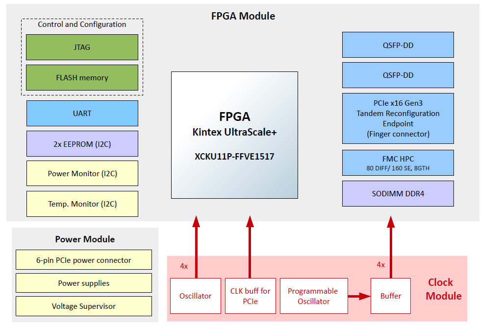
FPGA1 – Kintex Ultrascale+ XCKU11P-FFVE1517 |
PCIe x16 gen3 endpoint or PCIe x8 gen4 | ||
| 2x QSFP-DD (total up to 400Gbps) | |||
| Power | |||
| Standard 6-pin PCIe power supply connector for system powering | |||
| Can be powered from PCIe finger connector in low power consumption systems (without FMC and QSFP) | |||
| Power supply voltages supervisor | |||
| I2C power and current measurements | |||
| Global Clock | Miscellaneous | ||
| Programmable oscillator for QSFP-DD |
FMC HPC standard connector VITA 57.1-2010 compliant (160 SE / 80 DIFF IOs and 8x GTY Links) |
||
| 4x Oscillators | UART | ||
| Dedicated clock buffer for PCIe interface | Temperature Sensor | ||
| Memory | Battery for BBRAM Encrypted Key Storage | ||
| SODIMM DDR4 Memory socket | Configuration | ||
| 512 Mb Flash Memory | Flash memory with Tandem PROM function | ||
| 2x 64 kb I2C EEPROM | JTAG interface | ||
HES-XCKU11P-DDR4
FPGA & Capacity
- Main FPGA: Kintex Ultrascale+ XCKU11P-FFVE1517
- 653K Logic Cells
- 21.1 Mb Total Block RAM
- 22.5 Mb Total UltraRAM
- 2,928 DSP Slices
Memory Resources
- SODIMM DDR4 Memory socket
- 512 Mb Flash Memory
- 2x 64 kb I2C EEPROM
Global Clock
- Programmable oscillator for QSFP-DD
- 4x Oscillators
- Dedicated clock buffer for PCIe interface
Interfaces & Hosting:
- PCIe x16 gen3 endpoint or PCIe x8 gen4
- 2x QSFP-DD (total up to 400Gbps)
Power
- Standard 6-pin PCIe power supply connector for system powering
- Can be powered from PCIe finger connector in low power consumption systems (without FMC and QSFP)
- Power supply voltages supervisor
- I2C power and current measurements
Miscellaneous
- FMC HPC standard connector VITA 57.1-2010 compliant (160 SE / 80 DIFF IOs and 8x GTY Links)
- UART
- Temperature Sensor
- Battery for BBRAM Encrypted Key Storage
Corporate Headquarters
2260 Corporate Circle
Henderson, NV 89074 USA
Tel: +1 702 990 4400
Fax: +1 702 990 4414
https://www.aldec.com
©2024 Aldec, Inc.