FMC-PCIe High-Bandwidth, High Throughput Serial Bus Daughter Card
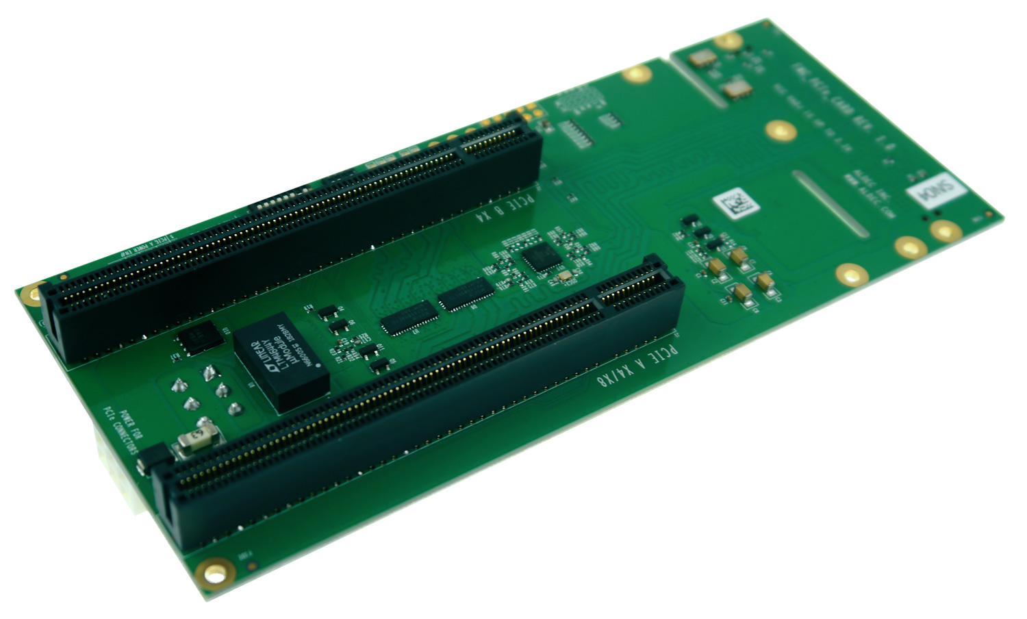
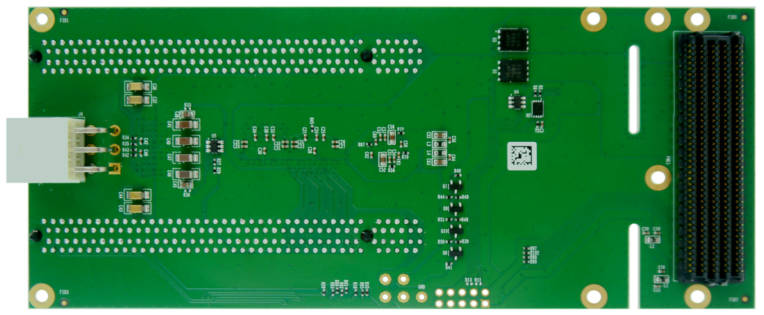
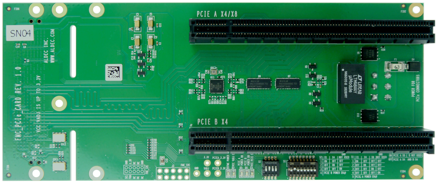
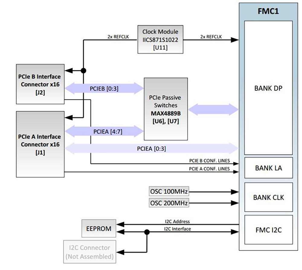
FMC-PCIe expansion daughter card can be used as PCIe root complex and provided two PCIe x4 interfaces or one PCIe x8 interface for endpoints cards equipped with standard PCIe finger connector up to x16. This board includes two PCIe connectors on the bottom. There are Four PCIe lines which are switched between two PCIe connectors using passive switches on the board. The 100MHz reference clocks for PCIe and FMC connectors are generated using LVDS oscillators on the FMC-PCIe card. This board needs to be powered up using an external 12V power supply with 6-pin PCIe power connector.
Some of the use cases board would be in High Performance Computing (HPC) applications that high speed and high bandwidth data transferring is required. The FMC-PCIe daughter card is designed based on Vita 57.1 standard and is supported by Aldec TySOM™ embedded development cards and HES™ prototyping boards.
FMC-PCIe High-Bandwidth, High Throughput Serial Bus Daughter Card
Components & Interfaces
- FMC HPC standard connector compliant with VITA 57.1-2010
- PCIe Interface x4 or x8 (connector x16)
- PCIe Interface x4 (connector x16)
Memory
- 64 kb EEPROM for FMC standard I2C Bus
Miscellaneous
- 2x Oscillators (100MHz, 200MHz)
- 100MHz Reference Clocks for PCIe interfaces
Corporate Headquarters
2260 Corporate Circle
Henderson, NV 89074 USA
Tel: +1 702 990 4400
Fax: +1 702 990 4414
https://www.aldec.com
©2024 Aldec, Inc.