Aldec cuts ASIC design prototype bring-up time with HES-DVM’s automatic partitioning tool and faster HDL-to-FPGA compilation times
The 2019.09 release of HES-DVM provides fast compilation and FPGA partitioning automation, aiding greatly in design setup for physical prototyping on multi-FPGA boards from Aldec and some third-party boards
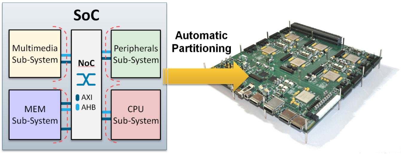
Henderson, NV, USA – September 24, 2019 – Aldec, Inc., a pioneer in mixed HDL language simulation and hardware-assisted verification for ASIC and FPGA designs, has introduced automatic FPGA partitioning to its popular HES-DVM™; the company’s fully automated and scalable hybrid verification environment for SoC and ASIC designs.
Traditionally, and subject to design complexity and constraints, the manual partitioning of multiple FPGAs used for prototyping can take days, or even weeks, whereas the automation in HES-DVM can perform the task in minutes; ideal for exploratory, What-If scenarios.
The latest release of HES-DVM, 2019.09, also features Aldec’s proprietary HDL compiler. Called SyntHESer, and announced earlier this year, in a recent in-house bench test, the compiler performed 10x faster than a leading standalone synthesis tool, when handling identical blocks of HDL for a circa 45-million-gate Deep Learning Accelerator (DLA) design.
“These additions to HES-DVM rise to some of the biggest challenges associated with the FPGA-based prototyping of an ASIC design,” said Zibi Zalewski, General Manager of Aldec’s Hardware Division. “With the 2019.09 release of HES-DVM, the most tedious and challenging activities, such as creating and matching partitions with on-board FPGAs or assigning limited FPGA I/O resources, are fully automated.”
For the 2019.09 release of HES-DVM, Aldec engineers designed and implemented fast and efficient algorithms capable of finding balanced partitions and minimizing required interconnections.
“The user can jump into the process of partitioning any time and modify the partitions and interconnections in harmony with automation algorithms,” adds Zalewski.
Lastly, but by no means of least importance, HES-DVM sees the introduction of Board Compiler, used to import files, in the form of Verilog structural descriptions, for third party boards that use Xilinx Virtex® UltraScale™ devices. With this capability the user can easily reconfigure prototyping board by adding or removing inter-FPGA connections or creating hybrid configurations of tail (or daughter) boards and backplanes.
Zalewski concludes: “We are extremely proud of all these enhancements to HES-DVM, as they all set out to save engineers time without reducing their confidence in their design before they enter the next phase of the ASIC or SoC design lifecycle. Also, by introducing Board Compiler, which was done in response to user requests, we have increased the versatility of HES-DVM, so that it can be used with other boards.”
The 2019.09 software release of HES-DVM 2019.09 is available now. To learn more or to evaluate HES-DVM, please visit www.aldec.com, e-mail sales@aldec.com, call +1 (702) 990-4400, or contact one of Aldec’s worldwide distribution partners.
Aldec cuts ASIC design prototype bring-up time with HES-DVM’s automatic partitioning tool and faster HDL-to-FPGA compilation times.
About HES™ Prototyping
Aldec offers a portfolio of HES™ prototyping boards based on the largest Xilinx FPGAs of the Virtex UltraScale and Virtex-7 families. The boards are architected to allow for easy expansion using BPX backplane and standardized FMC and BPX daughter card connectors.
About HES-DVM™
HES-DVM™ is a fully automated and scalable hybrid verification environment for SoC and ASIC designs. Utilizing the latest co-emulation standards like SCE-MI or TLM and the newest FPGA technology, hardware and software design teams obtain early access to the hardware prototype of the design. HES-DVM is used in labs worldwide for all kinds of emulation and physical prototyping tasks including Simulation Acceleration, Hybrid Virtual Prototypes, In-Circuit Emulation, Software Validation and Prototyping.
About Aldec
Established in 1984, Aldec is an industry leader in Electronic Design Verification and offers a patented technology suite including: RTL Design, RTL Simulators, Hardware-Assisted Verification, SoC and ASIC Prototyping, Design Rule Checking, CDC Verification, IP Cores, High-Performance Computing Platforms, Embedded Development Systems, Requirements Lifecycle Management, DO-254 Functional Verification and Military/Aerospace solutions. www.aldec.com
Corporate Headquarters
2260 Corporate Circle
Henderson, NV 89074 USA
Tel: +1 702 990 4400
Fax: +1 702 990 4414
https://www.aldec.com
©2024 Aldec, Inc.